The SAMPULSE50GHz and SAMPULSE70GHzANT are demonstration boards for Furaxa InP single channel sampler/pulser ICs. The SAMPULSE50GHz model contains a 2.4mm combined TDR input/output connector to the common sampler/pulser node in the IC. The SAMPULSE70GHzANT is similar, except that instead of a single-ended 2.4mm connector, the sampler IC's differential inputs are fed from a bowtie antenna. In both models, the IC's differential sampler output is converted, using an AD8009 op amp, into a single-ended ground-referenced output that is sent to an SMA jack labeled SAMPLER OUTPUT.
The sampler clock input is fed into the SMA jack labeled SAMPLER CLOCK, and should ideally be a square wave with rise time under 150pS and amplitude of approximately 1V to 1.5V p-p. It may be set to any frequency from 1 MHz to 3GHz (a +12dBm sine wave input with approximately a 50% duty cycle may be substituted for the square wave for frequencies above 200MHz), causing the board take samples at rates from 1 million to 3 billion per second. Amplitude of either sine or square wave sampler clock input should be approximately +12dBm (~850mV RMS). The module is calibrated at the factory using a 1GHz sampler clock frequency. If changing sampler frequency outside the 1GSPS to 2GSPS range, it will be necessary to readjust potentiometer SVG3 as shown in Figure 2.
An optional pulser clock input is fed into the SMA jack labeled PULSER CLOCK IN, and may be set to any frequency from 1 MHz to 3GHz. It should ideally be a 1V p-p square wave with rise time under 150pS and duty cycle of approximately 50% (a +6dBm to +12dBm sine wave input may be substituted for the square wave for frequencies above 200MHz). Each PCLK transition causes the board to produce a pulse on the sampler/pulser node, which then appears at the 2.4mm sampler/pulser TDR input/output connector where it can be used to stimulate an external device-under-test (DUT), while the board's sampler can concurrently view this pulse and its reflections, as well as any additional signal emitted from the external DUT. When the pulser is not used, the board's negative power supply should be reduced to -5V (from its default value of -7V) so as not to couple in any noise that is generated by the pulser in the absence of a valid pulser clock.

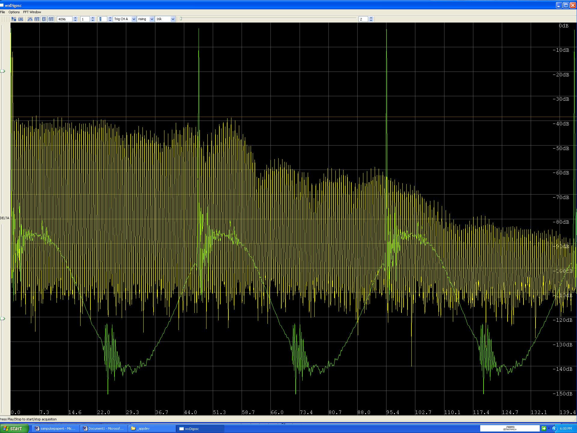
Figure 1. Usable sampler bandwidth and pulser energy to over 100GHz
SAMPLER SPECIFICATIONS:
- Sample rate: 1MSPS to 3000MSPS (clock sources under 200MHz must be square wave)
- Number of channels: 1
- Full Scale Input range: +/- 200mV (DO NOT EXCEED +/- 300mV)
- 3dB Input Bandwidth: 50 GHz / 70GHz
- 6dB Input Bandwidth: 70 GHz for 50GHz model
- Usable Bandwidth while maintaining 40dB SNR: 70 GHz
- SFDR: 30dB at maximum input level
- Dynamic Range: 85dB typical, 2MHz to 50GHz
- Input connector type: 2.4MM Jacks
- Output connector type: Two SMA connectors:
- Output signal +/- 1V peak into 50 ohms.
- IF output bandwidth: DC to 100MHz
PULSER SPECIFICATIONS:
- Pulser clock inputs: AC coupled, amplitude 500mV p-p to 1200mV p-p.
- Pulse repetition rate: 1MPPS to 3000MPPS (clock sources under 200MHz must be square wave with <150ps rise time - slower rise times will result in broader or nonexistant output pulse and/or added jitter)
- Pulse amplitude (pulser may be disabled): Adjustable from approximately 30mV to 300mV
- Pulse width, at 2.4mm input/output connector: Approximately 12ps, viewed on HP 54750/54752A scope.
Demo Board Power Requirements:
- +4.6V (5V acceptable) at 80mA (typical), -5V at 150mA (typical) when using sampler only. Negative supply must be set to -7V, and valid pulser clock applied, if using pulser.